
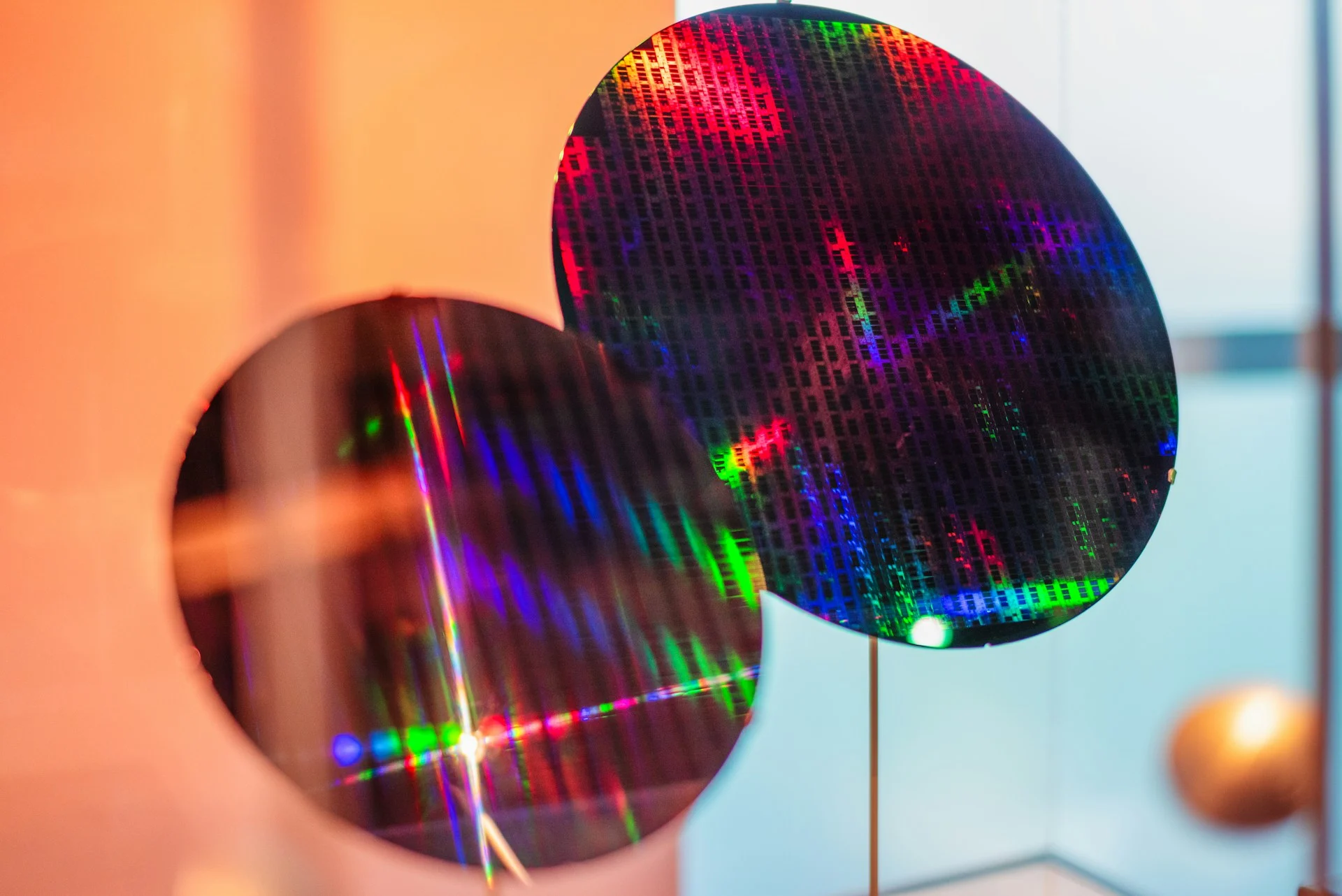
Every AI chatbot answer you get depends on memory chips stacked next to a GPU, and a lot of that memory is now coming from rice-paddy country south of Seoul. Samsung Pyeongtaek, a chip campus roughly the size of New York’s Central Park, runs three fabs around the clock, is bringing a fourth online and is building a fifth that could become the largest single chip plant on Earth.
The scene was described on 20 October 2026 in a dispatch by Michelle Kim for MIT Technology Review. Here’s what is being built, why, and what it means for the AI boom.
Key takeaways
- Samsung Pyeongtaek has three fabs running nonstop and a fourth (P4) coming online, with a fifth (P5) under construction.
- The expansion is Samsung’s bid to win back the lead in high-bandwidth memory (HBM) from SK Hynix, which has been Nvidia’s main supplier.
- P5 is reported to cost around 60 trillion won and is targeted for operation in 2028.
- Samsung’s HBM4 yield has reportedly climbed to nearly 80%, up from below 60% when mass production began in February 2026.
- Even with all this, large amounts of new memory supply are not expected before 2028.
What is Samsung building at Pyeongtaek?
A fab is a chip factory: a building wrapped around a cleanroom, where silicon wafers move through hundreds of steps in air far cleaner than an operating theatre. Pyeongtaek is Samsung’s newest and biggest cluster of them.
According to TrendForce, citing Korean media in August 2026, P4 uses a “double-fab” design with four cleanrooms in one building, and Samsung is fitting it with a 1c DRAM line. 1c is its newest DRAM process, used for its latest HBM products.
P5 is even bigger. Samsung has asked to raise the site’s floor area limit so that P5-1 and P5-2 can each use a triple-fab design. If approved, P5 would hold up to six cleanrooms and more than 1.5 times P4’s output.
Samsung Pyeongtaek fab by fab: where each line stands
| Line | Status (as of October 2026) | What it is for |
|---|---|---|
| P1 to P3 | Running around the clock | Memory and other chips |
| P4 | Coming online; double-fab, four cleanrooms | 1c DRAM for latest HBM |
| P5-1 and P5-2 | Foundation work under way; operation targeted for 2028, full completion 2030 | HBM, high-end DRAM, next-gen V-NAND, advanced foundry |
P5 has a stop-start history. Construction began in 2022, then Samsung paused it during the 2024 slump in memory demand. The AI boom brought it back to life.
Why does AI need so much memory?
AI models run on GPUs, but a GPU is only as fast as the data it can reach. High-bandwidth memory solves that by stacking DRAM chips vertically, like floors in a tower, and packaging them right beside the processor.
Think of the GPU as a chef and HBM as the counter beside the stove. A bigger, closer counter means less running to the pantry. Every new generation of Nvidia accelerator wants a bigger counter.
That is why memory has become the bottleneck. In a December 2025 report, TrendForce said Samsung aimed to lift HBM capacity to about 250,000 wafers a month by the end of 2026, from roughly 170,000. That is close to a 50% jump in a single year.
Can Samsung catch SK Hynix?
For most of the AI boom, Samsung’s smaller rival SK Hynix led in HBM for Nvidia’s accelerators. TSMC, meanwhile, dominates foundry work, which means making chips that other companies design. Pyeongtaek is Samsung’s attempt to take back the top spot in memory.
The signs are improving. Samsung began HBM4 mass production in February 2026, and its yield (the share of chips that come out working) has reportedly risen from below 60% to nearly 80%. Higher yield means more sellable chips from the same wafers, which matters as much as building new fabs.
The money is huge. In November 2025 Samsung pledged 450 trillion won (about $309 billion) for South Korea over five years, with P5 construction due to finish in 2027 and commercial operation in 2028. It is also breaking ground on a separate 6 trillion won HBM fab at its Onyang campus.
My take: capacity alone won’t settle this. SK Hynix is also building triple-fab plants at its Yongin cluster. The winner will be whichever company turns cleanroom space into Nvidia-approved stacks fastest.
Who is actually building it?
Thousands of workers, many brought in by shuttle bus from the older Songtan district nearby. MIT Technology Review spoke to Choi Hye-rin, a 35-year-old safety officer who supervises a crew building cable ducts and earns 140,000 won (about $97) a day.
“The rate here is higher than other construction sites, and the work is relatively easy.”
Choi Hye-rin, safety officer, to MIT Technology Review
Hundreds of women work on site, many as spotters who walk ahead of heavy machinery. Banners read “Even if the work runs late, don’t rush.” Helmets carry the pledge “I will not work if it’s not safe.” Those are small details, but they show a build pushing hard against its deadlines.
What happens next
- P4 ramp: Samsung aims to get its 1c DRAM line producing HBM at scale through late 2026 and into 2027.
- P5 approval: the floor-area change for the triple-fab design still needs approval. Operation is targeted for 2028.
- Supply stays tight: new fabs usually take more than three years from groundbreaking to wafer shipments, so big new supply is unlikely before 2028.
- The demand question: Samsung expects memory demand to keep rising through 2028. If AI spending cools, as it did with memory in 2024, the build-out could slow again.
The chip race is not only about hardware. Cloud companies are also trying to cut their reliance on Nvidia, as we covered in Amazon TorchNeuron: The Free Tool Aimed at Nvidia’s CUDA Moat.
FAQ
Where is Samsung Pyeongtaek?
It is in Pyeongtaek, a farming city south of Seoul, South Korea. The campus covers an area about the size of Central Park.
What is HBM and why does it matter?
High-bandwidth memory is a stack of DRAM chips packaged right beside a GPU. It feeds data to AI processors fast enough to keep them busy, and it is one of the main bottlenecks in AI hardware supply.
When will Pyeongtaek’s fifth fab open?
Samsung has said P5 construction should end in 2027 with commercial operation in 2028. Full completion of the P5 complex is targeted for 2030.
Want to know where the AI boom is really bottlenecked? Watch HBM yields and fab start dates, not just GPU launches, and follow Nerdlyst for the next chapter.
2 comments